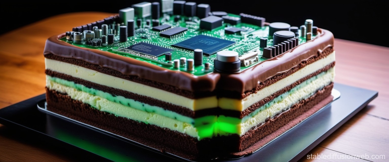
When you have a diverse team of experienced engineers, it can be hard to find efficient ways to share knowledge broadly. Yet, there is just too much valuable expertise not to. To capture 219’s electrical engineers’ shortcuts and best practices, we decided to test a new method for next level knowledge sharing. It’s a piece of CAKE!
How Do You Share Knowledge?
When it comes to Altium, all members of our electrical engineering team are very capable of bringing a design to life. But, we each have tips and tricks to complete a design quicker or at a higher quality that not everyone is aware of. That’s where CAKE comes in – for times when traditional solutions like presentations and working in pairs aren’t efficient options.
What is CAKE?
Is it CAKE? Yes, but sadly not the kind you can eat. The acronym stands for Collaborative Altium Knowledge Exchange. AI acronyms for the win!
CAKE is an exercise to efficiently share the various ways team members use Altium. With a program like Altium, there is always another tool, dropdown, or shortcut to discover. Using this exercise, junior and senior engineers alike can learn from each other.
It’s As Easy as 1-2-3
- First, a member of the team creates a hand-drawn circuit to share. It doesn’t need to be complicated. A very simple circuit will keep the implementation quick while providing insight into an individual’s Altium workflow.
- Next, each team member implements the circuit in Altium (schematic, layout, and design release). Use Loom to record screen and narration while completing the exercise. Bonus points for using Keyviz to make your keypresses visible so team members can learn your keyboard shortcuts!
- Finally, share the videos for the team to watch on their own schedule, at up to 2.5x speed.
Our CAKE Exercise
Below are some of the learnings from our own internal CAKE exercise. Your team will have your own unique set of learnings.
| Action/Tool | Benefits | Implementation |
| Turn on Cross Select Mode | Visualize selected components across schematic and layout. | Tools → Cross Select Mode |
| Center Reference Designators within their footprints | Keep reference designators visible but out of the way for initial component placement. | On the layout, Ctrl+ A to select all. In the properties tab, filter to only include Components. Then click on Designator to open the Designator properties. Then set Autoposition to Center. |
| Add Stitching Vias | Quickly add stitching vias to a net to ensure clean return paths, avoid ground loops, improve heat dissipation, and reduce noise. | Right click on PCB → add stitching vias → select net |
| Create Polygon Pours based on the board outline | Quickly create full pours without having to trace the board outline. | Tools → Polygon Pours → Polygon Pour Manager → New Polygon from… → Board Outline |
| Unlock a Footprint’s Primitives | Helpful to remove silk markings within a footprint that might be violating design rules. | Select the part, in the properties tab, click the Primitives lock icon to unlock. Then move or remove desired primitives. Then reselect the part and click the icon again to relock. |
| View the Bare 3D PCB | See any possible issues with the bare board that may be visibly blocked by 3D models in the full 3D mode. | When 3D mode is active, press Shift + z to view the bare PCB. |
| Move a Part while ignoring the snapping grid | Keep your rough snapping grid in place for most components while being able to quickly place more precise components off of the snapping grid. | Hold Ctrl while moving a part to ignore snapping guides. |
| Incrementally Place a Selected Group of Parts | Increases part placement speed by reducing clicks. Especially useful for large amounts of passive components. | Select a group of passives (a block) then press T > O > L to incrementally place each. |
| Set Menus to Popup Mode | Maximized working area during layout, which is helpful when working on a small screen. | On a panel, click the pin icon in the upper right hand corner. A vertical pin means the panel is in dock mode. A horizontal pin means the panel is in popup mode. Altium documentation |
| Fanout Components | Fanout all component pads for easier trace placement. Especially useful for tight spacing such as BGA routing. Also, helps easily connect pads that connect to power plane nets. | Route → Fanout Altium documentation |
| ActiveRoute | Use the ease of an auto-router with the control of manual placement by using ActiveRoute on a single trace, component, or layer. | View → Panels → PCB ActiveRoute Altium documentation |
| Re-route Component | Automatically re-draw attached tracks while nudging components. | Preferences → PCB Editor → Interactive Routing → Select Component re-route checkbox |
| Gloss Routing | Glossing will clean up traces by reducing length and corners and setting the corner shape. | Gloss while routing Preferences → PCB Editor → Interactive Routing → Set Gloss Effort (Routed) to Off/Weak/Strong Gloss existing routing Route → Gloss Selected Altium documentation |
| Silkscreen Cleanup | Quickly move silkscreen off of pads and vias. | Tools → Silkscreen Preparation |
| Outline Tracks or Text | Create single click guard rings or emphasis tracks or text with silkscreen outlines. | Tools → Outline Selected Objects |
Next Steps
Interested in next-level knowledge sharing via the CAKE exercise? Just come up with your own simple circuit to try and then compare notes!
If you have a PCB you need designed (or other custom electronics) and don’t want to do it yourself, reach out to 219’s electrical design team at getstarted@219design.com!
Photo Credit: Stable Diffusion Web
